By combining atomically thin devices with conventional microchips, scientists have created brain-mimicking hybrid electronics that can help implement neural-network artificial-intelligence systems in a far more energy-efficient way than standard electronics, a new study finds.
As electronics become tinier and tinier, scientists are investigating atomically thin 2D materials for next-generation electronics. For example, graphene consists of single layers of carbon atoms, and molybdenum disulfide is made of a sheet of molybdenum atoms sandwiched between two layers of sulfur atoms.
“Two-dimensional materials not only have state-of-the-art electrical performance but also have outstanding thermal, mechanical, optical, and chemical properties, which could result in novel applications that now don’t exist,” says study senior author Mario Lanza, an associate professor of materials science and engineering at King Abdullah University of Science and Technology, in Thuwal, Saudi Arabia.
“Most people’s expertise is in semiconductors. We are experts in insulators.”
—Mario Lanza, King Abdullah University of Science and Technology
Multiple research teams have developed prototype devices based on 2D materials. However, none have displayed the ability to compute or store data. In addition, their fabrication mostly relied on synthesis and processing methods that are not compatible with standard industry techniques. Furthermore, manipulating single-layer 2D materials is challenging because defects can occur when transferring them from the surfaces on which they are grown onto substrates more useful for applications. These defects reduce device consistency and yield.
Now scientists have created what they say is the first densely integrated microchip fabricated with 2D materials, all using processes compatible with the semiconductor industry. “We not only achieved excellent properties but also high yield and low variability,” Lanza says.
In the new study, researchers experimented with hexagonal boron nitride. This atomically thin ceramic often finds use as an insulating material in 2D electronics. “Most people’s expertise is in semiconductors,” Lanza says. “We are experts in insulators.”
The scientists wanted to overcome a number of challenges faced by previous devices based on 2D materials. For example, instead of seeking to fabricate transistors from the 2D materials, Lanza and his colleagues aimed to create memristors. Memristors, or memory resistors, are essentially switches that can remember which electric state they were toggled to after their power is turned off.
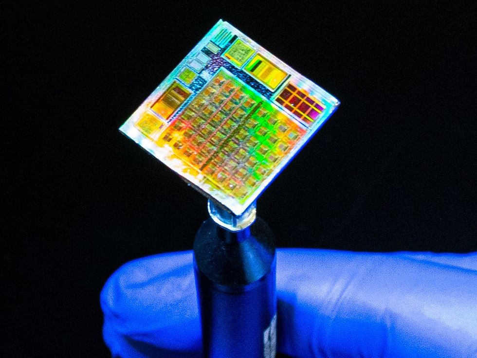 This hybrid 2D/CMOS microchip shows promise for memristive applications.Mario Lanza
“Most groups are focused on transistors, probably because they are the flagship components of electronics,” Lanza says. “Instead, we focused on memristors, which currently have a much smaller market size but also have tremendous potential for data storage, computation, encryption, and communication.”
Scientists worldwide hope to use memristors and similar components to build electronics that, like neurons, can both compute and store data. These memristive devices may greatly reduce the energy and time lost when conventional microchips shuffle data back and forth between processors and memory. Such brain-inspired neuromorphic hardware may also prove ideal for implementing neural networks. These AI systems are increasingly finding use in applications such as supporting autonomous vehicles and analyzing medical scans.
Memristors are “simple devices that are defect-tolerant,” Lanza says. In contrast, transistors “require perfect crystalline material,” he explains. Lanza notes that memristors also don’t suffer from other problems that transistors do, such as contact resistance—that is, electrical resistance at their points of contact with other components.
In addition, where most prior work relied on 2D materials that were just one or two layers thick, Lanza and his colleagues used a sheet of 2D material consisting of roughly 18 layers that was altogether about 6 nanometers thick. “This thicker material is not so easy to crack,” Lanza says.
Moreover, instead of building 2D devices on top of a blank substrate such as a conventional silica-silicon wafer, the researchers fabricated their 2D devices on top of standard CMOS microchips. The microchips can help control electric current and switching in the memristors, which helped lead to successful 2D devices.
Researchers fabricating transistors for computation typically use so-called front-end-of-line steps. In contrast, Lanza and his colleagues built their memristors on the back-end-of-line interconnections that link devices on wafers. Memristors are normally integrated onto microchips this way, “with the difference that we used 2D materials instead of other materials,” Lanza says.
The researchers transferred a multilayer sheet of hexagonal boron nitride onto the back-end-of-line interconnections of 4-square-centimeter silicon microchips containing CMOS transistors of the 180-nanometer node on a 200-millimeter silicon wafer. They next fabricated circuits from this combination by etching the hexagonal boron nitride and patterning and depositing electrodes on top. These circuits each consisted of 5-by-5 crossbar arrays of cells, each made up of one transistor and one memristor.
Whereas most devices made using 2D materials are more than 1 square micrometer in size, the memristors in the new study are only 0.053 µm2, the researchers note. These memristors “could be made much smaller very easily if more advanced microchips were available,” Lanza says.
The CMOS transistors helped control the electrical currents across the 2D memristors. This helped achieve memristor endurances of about 5 million cycles of switching, roughly on par with existing resistive RAM and phase-change memories. Without the CMOS transistors, the memristors endured only about 100 cycles.
The researchers showed they could perform in-memory computing operations with their device, constructing “or“ and “imply“ logic gates. They note they could run more sophisticated operations by modifying the interconnections between the devices.
In addition, the scientists note the electrical conductivity of the hybrid microchip could be dynamically adjusted to different levels by applying electrical pulses, a property called spike-timing dependent plasticity. This feature suggests that the device could help implement spiking neural networks that more closely imitate the human brain than conventional neural networks do.
The key components in a spiking neural-network “spike”—that is, generate an output signal—only after they receive a certain amount of input signals over a given time. Since spiking neural networks only rarely fire spikes, they shuffle around much less data than typical artificial neural networks and in principle require much less power and communication bandwidth. Conventional electronics are not well-suited for running spiking neural networks, resulting in a market need to develop new neuromorphic hardware to run them, the scientists note.
As a proof of principle, the researchers created a spiking neural network using their device that had 784 input neurons, an excitatory layer of 400 neurons, and an inhibitory layer of 400 neurons. When tested with a standard task—classifying the images from the Modified National Institute of Standards and Technology (MNIST) database of handwritten digits—this simple device nevertheless achieved roughly 90 percent accuracy.
The scientists note that their devices need about 1.4 to 5 volts for switching, which is low compared with other prototypes in the field of 2D materials, which may require more than 20 V. Still, they note this voltage is higher than that used at the 180-nm CMOS node. However, they suggest this voltage may not impede the development of this technology, as there are many commercial microchips that operate at much higher voltages—for instance, state-of-the-art 3D-NAND Flash memories are programmed at roughly 20 V, and all bipolar-CMOS microchips for automotive applications require up to 40 V.
Previously, IBM researchers experimented with the benefits of placing 2D materials on a microchip. In 2011, they fabricated a circuit that contained one graphene transistor and two inductors, and in 2014 developed a larger circuit with three graphene transistors, four inductors, three capacitors, and two resistors, Lanza says. However, IBM apparently abandoned this approach, “probably because of the difficulties of transferring a monolayer 2D material,” he says. In contrast, Lanza and his colleagues used a more durable, 18-layer-thick material. He predicts “now many other scientists will create their prototypes on functional microchips instead of nonfunctional SiO2 substrates, which will provoke many more findings.”
Lanza also notes that 2D materials are normally the province of materials scientists, not microchip engineers. “To do the experiment we did, you need to design a microchip using specific software, and then make a multiproject wafer tape-out or, as in our case, an entire wafer,” he says. “If you use CMOS technology of the 180-nm node, as in our case, the first costs US $25,000, the second one costs US $100,000. Many research groups not only cannot design this, they can’t even afford this. In our case, my colleagues at Tsinghua University provided the wafers and I integrated the material.”
Lanza notes that their research has already attracted the interest of leading semiconductor companies. The scientists now aim to move beyond 4 cm2 silicon microchips “to make entire 300-mm wafers,” Lanza says.
The scientists detailed their findings 27 March in the journal Nature.
Updated 6 April 2023